Beating the diffraction limit in diamonds

by Daniel Heimsoth

Resolving very small objects that are close together is a frequent goal of scientists, making the microscope a crucial tool for research in many different fields from biology to materials science.

The resolution of even the best modern confocal microscopes — a common optical microscope popular in biology, medicine, and crystallography — is limited by an optical bound on how narrow a laser beam can be focused, known as the diffraction limit.

In a study recently published in the journal ACS Photonics, UW–Madison physics professor Shimon Kolkowitz and his group developed a method to image atomic-level defects in diamonds with super-resolution, reaching a spatial resolution fourteen times better than the diffraction limit achievable with their optics. And, because the technique uses a standard confocal microscope, this super-resolution should be available to any researchers that already have access to this common equipment.
profile photo of Aedan Gardill
Aedan Gardill

While methods to achieve super-resolution already exist, such as stimulated emission depletion microscopy (STED), nearly all of these methods either require the addition of special optics, which can be expensive and difficult to install, or specialized samples and extensive post processing of the data. The UW–Madison technique, which they call “super-resolution Airy disk microscopy” (SAM), avoids such barriers to entry.

“You can get this all for free with the existing setup that a lot of labs already have, and it performs almost just as well,” says Aedan Gardill, a graduate student in Kolkowitz’s group and lead author of the paper. “We were able to get resolution down to twenty nanometers, which is comparable with standard techniques using [STED].”

The ‘Airy disk’ in SAM refers to a key feature of light beams that gives rise to the diffraction limit but which the researchers turned to their advantage.

Confocal microscopes use laser beams of specific wavelengths to excite matter in a sample, causing that matter to emit light. On the microscopic scale, the laser beam does not create a solid circle of light on the sample in the same way a flashlight would.  Rather, light hits the object in a series of light and dark rings called an Airy pattern. Within the dark rings, the matter receives no light, which means it cannot be detected by the microscope’s light sensors.

The novelty of the SAM technique is in its two laser beam pulses, one spatially offset from the other such that the overlapping Airy patterns can distinguish between two closely spaced objects.

In their paper, the research team studied nitrogen-vacancy (NV) centers in diamond crystal, which are regions in the crystal lattice where one of two neighboring carbon atoms is replaced by a nitrogen atom, and the other is left empty. NV centers are known to have two different charge states based on how many electrons are in the defect, one that fluoresces and one that remains dark when yellow light is applied to them.

To resolve two NV centers separated by a distance less than the diffraction limit of the microscope, the SAM procedure first shines green light on them, preparing both centers into their fluorescent charge state. Then, a red laser is applied, offset such that only one of the two NV centers is in the dark ring of the Airy pattern and thus is not affected by the beam. The NV center that does see the red light is switched to the dark state.
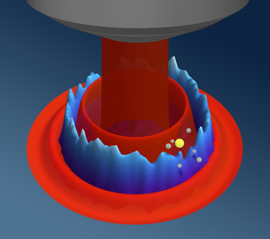
a cartoon-rendered image of a microscope objective, with a red cylinder (light) hitting a sample that shows concentric rings of red and blue, as described in the text
Super-resolution Airy disk Microscopy uses the Airy disk (red pattern) generated by diffraction from an objective lens aperture (gray cylinder) to localize and control an emitter (here a nitrogen vacancy center in diamond) below the diffraction limit. Emitter fluorescence is suppressed everywhere except in a very narrow ring (blue donut).

“It goes to another dark charge state where it does not interact with yellow light,” Gardill explains. “But the initial bright charge state does interact with yellow light and will emit light.”

Finally, when the yellow laser is applied, one NV center emits light while the other does not, effectively differentiating between the two neighboring sites. By repeating these steps iteratively over a grid, the researchers could reconstruct a full image of the two nearby NVs with spectacular resolution.

The idea for this technique came as a bit of a surprise while the team was studying charge properties of NV centers in 2020.

“We tried the combinations of red-green, green-red, red-red, green-green with those first two [laser] pulses, and the one that was green then red, we ended up seeing this ring,” Gardill recounts. “And Shimon was like, ‘The width of the ring is smaller than the size of [the confocal image of] the NV. That is super-resolution.’”

This method could find wide use in many different fields, including biology and chemistry where NV centers are used as nanoscale sensors of magnetic and electric fields and of temperature in compounds and organic material. NV centers have also been studied as candidates for quantum repeaters in quantum networks, and the research team has considered the feasibility of using the SAM technique to aid in this application. Currently, the SAM method has only been applied to NV centers in diamond crystal, and more research is needed to extend its use to different systems.

That all of this can be done with hardware that many labs across the world already have access to cannot be overstated. Gardill reiterates, “If they have a basic confocal microscope and don’t want to buy another super-resolution microscope, they can utilize this technique.”

This work was supported by the U.S. Department of Energy, Office of Science, Basic Energy Sciences under Award #DE-SC0020313.

Daniel Heimsoth is a second-year PhD student in Physics. This was his first news story for the department.

Welcome, assistant professor Ilya Esterlis

profile photo of Ilya Esterlis
Ilya Esterlis

When Lake Mendota freezes over in the winter and thaws in the spring, those water/ice phase transitions might seem mundane. But, says new assistant professor of physics Ilya Esterlis, interesting things happen during phase transitions, and commonalities exist between phase transitions of any matter.

“That’s very surprising and strange sounding, but it turns out that there’s a very general framework in which to understand [these commonalities],” Esterlis says. “It’s this notion of universality, and by studying phase transitions you’re simultaneously studying a very broad class of materials.”

Esterlis, a condensed matter theorist whose research focuses on materials and phase transitions, joins the department January 1, 2023. He is currently a postdoctoral fellow at Harvard, and joined us for a virtual interview earlier this fall.

Can you please give an overview of your research?

I am a condensed matter theorist, so I study materials, and in particular I try to classify different phases of matter and the phase transitions between those phases of matter. I’m mostly interested in electronic systems, where you have a large macroscopic number of interacting electrons and are trying to understand the kind of phenomena that can emerge when you have that large number of degrees of freedom interacting with one another. And a lot of these things are motivated by experiments — not all of them. There are some more academic questions that I’m interested in investigating and they’re a bit more formal. But I’m also motivated by interesting things that are happening in the lab. Part of my work is not only trying to characterize and understand phases of matter, but also trying to propose ways that different phases could be detected experimentally, how they would manifest themselves in different experimental signatures.

I’m also interested in superconductivity. My PhD work focused a lot on trying to understand the optimal conditions for making superconductors — if you could have every knob at your disposal, what would you do to optimize them? Optimize in this case means: make superconductors that exist at as high of a temperature as possible. Superconductivity is typically a low temperature phenomenon, so there’s a holy grail in condensed matter physics trying to make higher temperature superconductors. Part of my work has been organized around trying to understand what would be even in principle the optimal route towards achieving higher temperature superconductors.

Once you’re in Madison, what are one or two research projects you and your group will focus on?

I will focus a good amount of my research efforts on studying superconductivity, continuing this line of investigation into what the optimal conditions for superconductors are. If you had all the freedom in the world, how would you build the best superconductor that exists to high temperatures and under normal laboratory conditions? Not under extreme, unrealistic conditions but in an everyday parameter regime. And that involves understanding the superconducting state itself. Superconductors are a phase of matter that is distinct from, say, a metal, which is also a good conductor but not a superconductor. But oftentimes to understand superconductors better, one has to understand the state from which they came. That is to say, you take a metal and you cool it down to low temperatures and it goes from being a good conductor to a superconductor. To understand that superconductor, it’s often helpful to understand the metal from which it came at higher temperature. And sometimes those metals can be conventional, like copper wires, but sometimes they can be very unconventional metals and strange for various reasons. One open question is: what is the interplay between superconductivity and unusual metals? If you take a high temperature unusual metal, what is the kind of superconductor that it turns into at lower temperature? And unusual in this context means that it has some properties that are not typical to conventional metals. For instance, there’s predictions for how resistance changes with temperature in a conventional metal but unusual metals have rather different resistance behaviors.

What is your favorite element and/or elementary particle?

Helium is remarkable in that it has a number of unusual properties. For instance, if you cool it down to zero temperature it does not crystallize, it remains a liquid. That’s solely due to quantum mechanics, which is kind of an incredible thing. If you do make it crystallize by applying pressure, then that solid itself also has very interesting properties.

And my favorite elementary particle is the anyon. It’s not elementary, say, in the sense of electrons or quarks. But it’s this really remarkable thing that happens in condensed matter systems where if you take a macroscopic number of electrons and you subject them to a very large magnetic field, then a remarkable thing happens where the behavior of the system, as viewed kind of on macroscopic scales, does not look like the behavior of electrons, it really looks like the behavior of particles called anyons that have fractional electric charge. So they are elementary in condensed matter physics.

What hobbies and interests do you have? 

I really love to play music, guitar specifically. And I have two small kids, two daughters, and I just like hanging out with them.

Welcome, Roman Kuzmin, the Dunson Cheng Assistant Professor of Physics

profile photo of Roman Kuzmin
Roman Kuzmin

In the modern, cutting-edge field of quantum computing, it can be a bit puzzling to hear a researcher relate their work to low-tech slide rules. Yet that is exactly the analogy that Roman Kuzmin uses to describe one of his research goals, creating quantum simulators to model various materials. He also studies superconducting qubits and ways to increase coherence in this class of quantum computer.

Kuzmin, a quantum information and condensed matter scientist, will join the department as an the Dunson Cheng Assistant Professor of Physics on January 1. He is currently a research scientist at the University of Maryland’s Joint Quantum Institute in College Park, Md, and recently joined us for an interview.

Can you please give an overview of your research?

My main fields are quantum information and condensed matter physics. For example, one of my interests is to solve complicated condensed matter problems using new techniques and materials which quantum information science developed. Also, it works in the other direction. I am also trying to improve materials which are used in quantum information. I work in the subfield of superconducting circuits. There are several different directions in quantum information, and the physics department at Wisconsin has many of them already, so I will complement work in the department.

Once you’re in Madison and your lab is up and running, what are the first big one or two big things you want to really focus your energy on

One is in quantum information and quantum computing. So, qubits are artificial atoms or building blocks of a quantum computer. I’m simplifying it, of course, but there are environments which try to destroy coherence. In order to scale up those qubits and make quantum computers larger and larger — because that’s what you need eventually to solve anything, to do something useful with it — you need to mitigate decoherence processes which basically prevent qubits from working long enough. So, I will look at the sources of those decoherence processes and try to make qubits live longer and be longer coherent.

A second project is more on the condensed matter part. I will build very large circuits out of Josephson junctions, inductors and capacitors, and such large circuits behave like some many-body objects. It creates a problem which is very hard to solve because it contains many parts, and these parts interact with each other such that the problem is much more complicated than just the sum of those parts.

What are some applications of your work?

Of course this work is interesting for developing theory and understanding our world. But the application, for example for the many-body system I just described, it’s called the quantum impurity. One of my goals is to use this to create a simulator which can potentially model some useful material. It’s like if you have a quantum computer, you can write a program and it will solve something for you. A slide rule is a physical device that allows you to do complicated, logarithmic calculations, but it’s designed to do only this one calculation. I’m creating kind of a quantum slide rule.

What is your favorite element and/or elementary particle? 

So, I have my favorite circuit element: Josephson junction. (editor’s note: the question did not specify atomic element, so we appreciate this clever answer!). And for elementary particle, the photon, especially microwave photons, because that’s what I use in these circuits to do simulations. They’re very versatile and they’re just cool.

What hobbies and interests do you have?

I like reading, travelling, and juggling.

New technique reveals changing shapes of magnetic noise in space and time

This article was originally published by Princeton Engineering

Electromagnetic noise poses a major problem for communications, prompting wireless carriers to invest heavily in technologies to overcome it. But for a team of scientists exploring the atomic realm, measuring tiny fluctuations in noise could hold the key to discovery.

“Noise is usually thought of as a nuisance, but physicists can learn many things by studying noise,” said Nathalie de Leon, an associate professor of electrical and computer engineering at Princeton University. “By measuring the noise in a material, they can learn its composition, its temperature, how electrons flow and interact with one another, and how spins order to form magnets. It is generally difficult to measure anything about how the noise changes in space or time.”

Using specially designed diamonds, a team of researchers at Princeton and the University of Wisconsin–Madison have developed a technique to measure noise in a material by studying correlations, and they can use this information to learn the spatial structure and time-varying nature of the noise. This technique, which relies on tracking tiny fluctuations in magnetic fields, represents a stark improvement over previous methods that averaged many separate measurements.

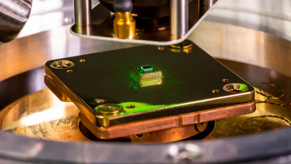
a small square chip sits on a metallic microscope stand with green laser light bouncing off of it in places
Using specially designed diamonds with nitrogen-vacancy centers, researchers at Princeton University and the University of Wisconsin-Madison have developed a technique to measure noise in a material by studying correlations, and they can use this information to learn the spatial structure and time-varying nature of the noise. In this image, a diamond with near-surface nitrogen-vacancy centers is illuminated by green laser light from a microscope objective lens | Photo by David Kelly Crow and provided by Princeton University

De Leon is a leader in the fabrication and use of highly controlled diamond structures called nitrogen-vacancy (NV) centers. These NV centers are modifications to a diamond’s lattice of carbon atoms in which a carbon is replaced by a nitrogen atom, and adjacent to it is an empty space, or vacancy, in the molecular structure. Diamonds with NV centers are one of the few tools that can measure changes in magnetic fields at the scale and speed needed for critical experiments in quantum technology and condensed matter physics.

While a single NV center allowed scientists to take detailed readings of magnetic fields, it was only when de Leon’s team worked out a method to harness multiple NV centers simultaneously that they were able to measure the spatial structure of noise in a material. This opens the door to understanding the properties of materials with bizarre quantum behaviors that until now have been analyzed only theoretically, said de Leon, the senior author of a paper describing the technique published online Dec. 22 in the journal Science.

“It’s a fundamentally new technique,” said de Leon. “It’s been clear from a theoretical perspective that it would be very powerful to be able to do this. The audience that I think is most excited about this work is condensed matter theorists, now that there’s this whole world of phenomena they might be able to characterize in a different way.”

One of these phenomena is a quantum spin liquid, a material first explored in theories nearly 50 years ago that has been difficult to characterize experimentally. In a quantum spin liquid, electrons are constantly in flux, in contrast to the solid-state stability that characterizes a typical magnetic material when cooled to a certain temperature.

profile photo of Shimon Kolkowitz
Shimon Kolkowitz

“The challenging thing about a quantum spin liquid is that by definition there’s no static magnetic ordering, so you can’t just map out a magnetic field” the way you would with another type of material, said de Leon. “Until now there’s been essentially no way to directly measure these two-point magnetic field correlators, and what people have instead been doing is trying to find complicated proxies for that measurement.”

By simultaneously measuring magnetic fields at multiple points with diamond sensors, researchers can detect how electrons and their spins are moving across space and time in a material. In developing the new method, the team applied calibrated laser pulses to a diamond containing NV centers, and then detected two spikes of photon counts from a pair of NV centers — a readout of the electron spins at each center at the same point in time. Previous techniques would have taken an average of these measurements, discarding valuable information and making it impossible to distinguish the intrinsic noise of the diamond and its environment from the magnetic field signals generated by a material of interest.

“One of those two spikes is a signal we’re applying, the other is a spike from the local environment, and there’s no way to tell the difference,” said study coauthor Shimon Kolkowitz, an associate professor of physics at the University of Wisconsin–Madison. “But when we look at the correlations, the one that is correlated is from the signal we’re applying and the other is not. And we can measure that, which is something people couldn’t measure before.”

Kolkowitz and de Leon met as Ph.D. students at Harvard University, and have been in touch frequently since then. Their research collaboration arose early in the COVID-19 pandemic, when laboratory research slowed, but long-distance collaboration became more attractive as most interactions took place over Zoom, said de Leon.

Jared Rovny, the study’s lead author and a postdoctoral research associate in de Leon’s group, led both the theoretical and experimental work on the new method. Contributions by Kolkowitz and his team were critical to designing the experiments and understanding the data, said de Leon. The paper’s coauthors also included Ahmed Abdalla and Laura Futamura, who conducted summer research with de Leon’s team in 2021 and 2022, respectively, as interns in the Quantum Undergraduate Research at IBM and Princeton (QURIP) program, which de Leon cofounded in 2019.

The article, Nanoscale covariance magnetometry with diamond quantum sensors, was published online Dec. 22 in Science. Other coauthors were Zhiyang Yuan, a Ph.D. student at Princeton; Mattias Fitzpatrick, who earned a Ph.D. at Princeton in 2019 and was a postdoctoral research fellow in de Leon’s group (now an assistant professor at Dartmouth’s Thayer School of Engineering); and Carter Fox and Matthew Carl Cambria of the University of Wisconsin–Madison. Support for the research was provided in part by the U.S. National Science Foundation, the U.S. Department of Energy, the Princeton Catalysis Initiative and the Princeton Quantum Initiative.

The University of Wisconsin–Madison’s Department of Physics contributed to this article.

Shimon Kolkowitz promoted to Associate Professor

profile photo of Shimon Kolkowitz
Shimon Kolkowitz

Congratulations to Shimon Kolkowitz on his promotion to Associate Professor of Physics with tenure! Professor Kolkowitz is an AMO physicist whose research focuses on ultraprecise atomic clocks and nitrogen vacancy (NV) centers in diamonds, both of which have applications in quantum sensing. He joined the UW–Madison physics faculty as an assistant professor in January 2018. Since then, he has published numerous articles in top journals, including incredibly accurate comparisons of the rate that clocks run this year in the journal Nature.

Department Chair Mark Eriksson emphasizes Kolkowitz’s contributions across all aspects of his work: “Shimon, graduate students, and postdocs here at Wisconsin, have set records with their atomic clock, and at the same time, Shimon has played critically important roles in teaching and service, including guiding our graduate admissions through the pandemic and all that entails.”

Kolkowitz has been named a Packard Fellow, a Sloan Fellow, and has earned an NSF CAREER award, amongst other honors. He is also the Education, Workforce Development, and Outreach Major Activities Lead for Hybrid Quantum Architectures and Networks (HQAN), an NSF QLCI Institute of which UW–Madison is a member.

Opening doors to quantum research experiences with the Open Quantum Initiative

This past winter, Katie Harrison, then a junior physics major at UW–Madison, started thinking about which areas of physics she was interested in studying more in-depth.

“Physics is in general so broad, saying you want to research physics doesn’t really cut it,” Harrison says.

She thought about which classes she enjoyed the most and talked to other students and professors to help figure out what she might focus on. Quantum mechanics was high on her list. During her search for additional learning opportunities, she saw the email about the Open Quantum Initiative (OQI), a new fellowship program run by the Chicago Quantum Exchange (CQE).

“This could be something I’m interested in, right?” Harrison thought. “I’ll apply and see what happens.”

What happened was that Harrison was one of 12 undergraduate students accepted into the inaugural class of OQI Fellows. These students were paired with mentors at CQE member institutions, where they conducted research in quantum science information and engineering. OQI has a goal of connecting students with leaders in academia and industry and increasing their awareness of quantum career opportunities. The ten-week Fellowship ran through August 19.

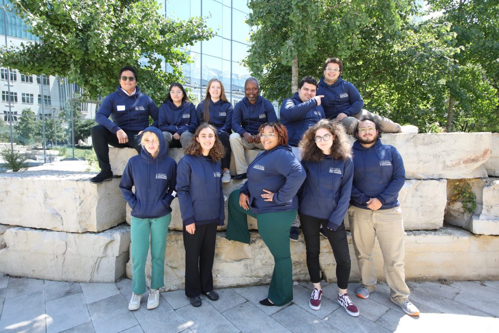
11 students pose on a rock wall, all students are wearing the same Chicago Quantum Exchange hooded sweatshirt
OQI students attend a wrap-up at the University of Chicago on August 17. Each student presented at a research symposium that day, which also included a career panel from leaders across academia, government, and industry and an opportunity to network. | Photo provided by the Chicago Quantum Exchange

OQI also places an emphasis on establishing diversity, equity, and inclusion as priorities central to the development of the quantum ecosystem. Almost 70% of this year’s fellowship students are Hispanic, Latino, or Black, and half are the first in their family to go to college. In addition, while the field of quantum science and engineering is generally majority-male, the 2022 cohort is half female.

This summer, UW–Madison and the Wisconsin Quantum Institute hosted two students: Harrison with physics professor Baha Balantekin and postdoc Pooja Siwach; and MIT physics and electrical engineering major Kate Arutyunova with engineering physics professor Jennifer Choy, postdoc Maryam Zahedian and graduate student Ricardo Vidrio.

Harrison and Arutyunova met at OQI orientation at IBM’s quantum research lab in New York, and they hit it off immediately. (“We have the most matching energies (of the fellows),” Arutyunova says, with Harrison adding, “The synergy is real.”)

Four people stand in a lab in front of electronics equipment
OQI Fellow Kate Arutyunova with her research mentors. (L-R) Engineering Physics professor Jennifer Choy, graduate student Ricardo Vidrio, Kate Arutyunova, and postdoc Maryam Zahedian. | Photo provided by Kate Arutyunova

Despite their very different research projects — Harrison’s was theoretical and strongly focused on physics, whereas Arutyunova’s was experimental and with an engineering focus — they leaned on each other throughout the summer in Madison. They met at Union South nearly every morning at 7am to read and bounce ideas off each other. Then, after a full day with their respective research groups, they’d head back to Union South until it closed.

Modeling neutrino oscillations

Harrison’s research with Balantekin and Siwach investigated the neutrinos that escape collapsing supernovae cores. Neutrinos have a neutral charge and are relatively small particles, they make it out of cores without interacting with much — and therefore without changing much — so studying them helps physicists understand what is happening inside those stars. However, this is a difficult task because neutrinos oscillate between flavors, or different energy levels, and therefore require a lot of time and resources to calculate on a classical computer.

Harrison’s project, then, was to investigate two types of quantum computing methods, pulse vs circuit based, and determine if one might better fit their problem than the other. Previous studies suggest that pulsed based is likely to be better, but circuit based involves less complicated input calculations.

“I’ve been doing calibrations and calculating the frequencies of the pulses we’ll need to send to our qubits in order to get data that’s as accurate as a classical computer,” Harrison says. “I’m working with the circuit space, the mathematical versions of them, and then I’ll send my work to IBM’s quantum computers and they’ll calculate it and give results back.”

While she didn’t fully complete the project, she did make significant progress.

“(Katie) is very enthusiastic and she has gone a lot further than one would have expected an average undergraduate could have,” Balantekin says. “She started an interesting project, she started getting interesting results. But we are nowhere near the completion of the project, so she will continue working with us next academic year, and hopefully we’ll get interesting results.”

Developing better quantum sensors 

Over on the engineering side of campus, Arutyunova was studying different ways to introduce nitrogen vacancy (NV) centers in diamonds. These atomic-scale defects are useful in quantum sensing and have applications in magnetometry. Previous work in Choy’s group made the NV centers by a method known as nitrogen ion beam implantation. Arutyunova’s project was to compare how a different method, electron beam irradiation, formed the NV centers under different starting nitrogen concentrations in diamond.

Briefly, she would mark an edge of a very tiny (2 x 2 x 0.5 millimeter), nitrogen-containing diamond, and irradiate the sample with a scanning electron microscope. She used confocal microscopy to record the initial distribution of NV centers, then moved the sample to the annealing step, where the diamond is heated up to 1200 celsius in a vacuum annealing furnace. The diamonds are then acid washed and reexamined with the confocal microscope to see if additional NV centers are formed.

“It’s a challenging process as it requires precise coordinate-by-coordinate calculation for exposed areas and extensive knowledge of how to use the scanning electron microscope,” says Arutyunova, who will go back to MIT after the fellowship wraps. “I think I laid down a good foundation for future steps so that the work can be continued in my group.”

Choy adds:

Kate made significant strides in her project and her work has put us on a great path for our continued investigation into effective ways of generating color centers in diamond. In addition to her research contributions, our group has really enjoyed and benefited from her enthusiasm and collaborative spirit. It’s wonderful to see the relationships that Kate has forged with the rest of the group and in particular her mentors, Maryam and Ricardo. We look forward to keeping in touch with Kate on matters related to the project as well as her academic journey.

Beyond the summer fellowship

 Both Harrison and Arutyunova think that this experience has drawn them to the graduate school track, likely with a focus on quantum science. More importantly, it has helped them both to learn what they like about research.

“I would prefer to work on a problem and see the final output rather than a question where I do not have an idea of the application,” Arutyunova says. “And I realized how much I like to collaborate with people, exchange ideas, propose something, and listen to people and what they think about research.”

They also offer similar advice to other undergraduate students who are interested in research: do it, and start early.

“No matter when you start, you’re going to start knowing nothing,” Harrison says. “And if you start sooner, even though it’s scary and you feel like you know even less, you have more time to learn, which is amazing. And get in a research group where they really want you to learn.”

Coherent light production found in very low optical density atomic clouds

No atom is an island, and scientists have known for decades that groups of atoms form communities that “talk” to each other. But there is still much to learn about how atoms — particularly energetically excited ones — interact in groups.

In a study published in PRX Quantum, physicists from the University of Wisconsin–Madison observed communication between atoms at lower and lower densities. They found that the atoms influence each other at 100 times lower densities than probed before, exhibiting slow decay rates and emitting coherent light.

“It seems that (low-density) groups of excited atoms spontaneously organize to then produce light that is coherent,” says David Gold, a postdoctoral fellow in Deniz Yavuz’s group and lead author of the study. “These findings are pretty interesting from a basic science standpoint, and in terms of quantum computing, the takeaway is that even with very low numbers of atoms, you can see significant amounts of (these effects).”

A well-established property of atoms is found in electron excitation: when a specific wavelength of light hits an atom of a specific element, an electron is excited to a higher orbital level. As that electron decays back to its initial state, a photon of a specific wavelength is emitted. A single atom has a characteristic decay rate for that process. When groups of atoms are studied, their interactions are observed: the initial decay rate is very fast, or superradiant, then transitions to a slower, or subradiant, rate.

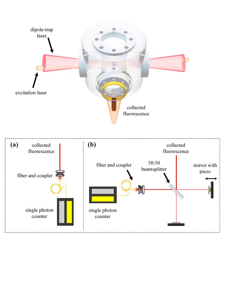
A schematic of the experimental setup. (Top) the overall apparatus used. (A) shows the setup for the first part of the experiment, where the researchers were measuring decay rates in lower and lower density clouds. (B) shows the setup for the second part of the paper, with the addition of an interferometer

Though well-established in dense clouds, this group-talk has never been studied in less dense clouds of atoms, which could have impacts on applications such as quantum computing.

In their first set of experiments, Gold and colleagues asked what the decay rate of lower-density clouds looked like. They supercooled the atoms in a cloud, hit them with an excitation laser, and recorded the decay rates as an intensity of emitted light over time. They observed the characteristic subradiance. In this case, they did not always see superradiance, likely due to the reduced number of atoms available to measure.

profile picture of David Gold
David Gold

Next, they asked what happened if they let the cloud expand — or decrease in density — for varying periods of time before repeating their experiment. They found that as the cloud become less and less dense, the amount of subradiance decreased, until eventually a density was reached where the atoms stopped behaving like a group and instead displayed single-atom decay rates.

“The most subradiance that we observed was at around a hundred times lower optical density than it had previously been observed before,” Gold says.

Now that the researchers knew that a less dense cloud still decays subradiantly to a point, they asked if the decay was happening in an isolated manner, or if the atoms were really acting as a group. If acting as a group, the emitted light would be coherent, or more laser-like, with some structure between the atoms.

They used the same experimental setup but added an interferometer, where light is split and recombined before the photons are detected. They first set the baseline interference pattern by moving the mirror closer or further away from the splitter — changing the path length of one of the beams — and mapping the interference pattern of the split light waves that were emitted from the same atom.

If there were no relationship between the two atoms and the light they emit, then they would have expected to see no interference pattern. Instead, they saw that for some distance of mirror displacement, the lightwaves did interfere, indicating that different atoms being measured were nonetheless producing coherent light.

“I think this is the more exciting thing we found: that the light that’s being emitted is coherent and it has more of the properties of a laser than you would expect,” Gold says. “The atoms are influenced by each other and not in a way we would have expected.”

Aside from the interesting physics seen in the study, Gold says the work is also applicable to quantum computing, particularly as those computers grow bigger in the future.

“Even if everything in a quantum computer is running perfectly and the system was completely isolated, there’s still this inherent thing of, well, the atoms just might decay down from [the computational] state,” Gold says.

This work was supported by National Science Foundation (NSF) Grant No. 2016136 for the QLCI center Hybrid Quantum Architectures and Networks.

UW–Madison, industry partners run quantum algorithm on neutral atom quantum computer for the first time

a quantum computing lab with lots and lots of wires and a main hardware piece in the center

A university-industry collaboration has successfully run a quantum algorithm on a type of quantum computer known as a cold atom quantum computer for the first time. The achievement by the team of scientists from the University of Wisconsin­–Madison, ColdQuanta and Riverlane brings quantum computing one step closer to being used in real-world applications. The work out of Mark Saffman’s group was published in Nature on April 20.

Read the joint press release

Read the press release tipsheet 

Undergraduate quantum science research fellowship launches

This story was originally published by the Chicago Quantum Exchange

The Open Quantum Initiative (OQI), a working group of students, researchers, educators, and leaders across the Chicago Quantum Exchange (CQE), announced the launch of the OQI Undergraduate Fellowship as part of their effort to advocate for and contribute to the development of a diverse and inclusive quantum workforce.

The primary mission of the OQI is to champion the development of a more inclusive quantum community. Science, technology, engineering, and mathematics (STEM) fields remain overwhelmingly white and male—only about 20% of bachelor’s degrees in physics, engineering, and computer science go to women, a mere 6% of all STEM bachelor’s degrees are awarded to African American students, and 12% of all STEM bachelor’s degrees are awarded to Hispanic students. But as the field of quantum science is still relatively new compared to other STEM subjects, groups like the OQI see a chance to make the foundations of the field diverse and accessible to all from the start.

“In many respects, we are building a national workforce from the ground up,” says David Awschalom, the Liew Family Professor in Molecular Engineering and Physics at the University of Chicago, senior scientist at Argonne National Laboratory, director of the Chicago Quantum Exchange, and director of Q-NEXT, a Department of Energy quantum information science center led by Argonne. “There are incredible opportunities here to make the field of quantum engineering as inclusive and equitable as possible from the very beginning, creating a strong ecosystem for the future.”

At the heart of the OQI’s effort is a new fellowship starting in summer 2022. For 10 weeks, fellows will live and work at a CQE member or partner institution, completing a research project in quantum information science and engineering under the guidance of a mentor. Students will have numerous opportunities to interact with the other fellows in their cohort during the summer research period and throughout the following academic year.

Through this fellowship, the students can expand their understanding of quantum science, receive career guidance, and grow their professional networks with leaders in academia and industry. The OQI will also aim to provide future research experiences in subsequent summers, as well as provide opportunities to mentor future fellows, helping to build a larger, diverse quantum community over time.

With the support of CQE’s member and partner institutions, including the University of Chicago, Argonne, Fermilab, University of Illinois Urbana-Champaign, University of Wisconsin-Madison, Northwestern University, and The Ohio State University, along with the NSF Quantum Leap Challenge Institute for Hybrid Quantum Architectures and Networks (HQAN) and Q-NEXT, this fellowship helps to establish diversity, equity, and inclusion as priorities central to the development of the quantum ecosystem.

The OQI launched the fellowship alongside a workshop on September 22 and 23. The OQI workshop, titled “Building a Diverse Quantum Ecosystem,” brought together CQE students, researchers, and professionals from across different institutions, including industry, to discuss the prevailing issues and barriers in quantum information science as the field develops. Institutional changemakers also shared what they have learned from their own efforts to increase representation. A panel on education and workforce development at the upcoming Chicago Quantum Summit on Nov. 4 will continue the discussion on building inclusive onramps for the quantum information science field.

“For quantum science and engineering to achieve its full potential, it must be accessible to all,” says Kayla Lee, Academic Alliance Lead at IBM Quantum and keynote speaker of the OQI workshop. “The OQI Undergraduate Fellowship provides explicit support for historically marginalized communities, which is crucial to increasing quantum engagement in a way that creates a more diverse and equitable field.”

Applications for the OQI Undergraduate Fellowship are open now.

a woman and a man in an optics lab adjust wiring and mirrors

Flexible, easy-to-scale nanoribbons move graphene toward use in tech applications

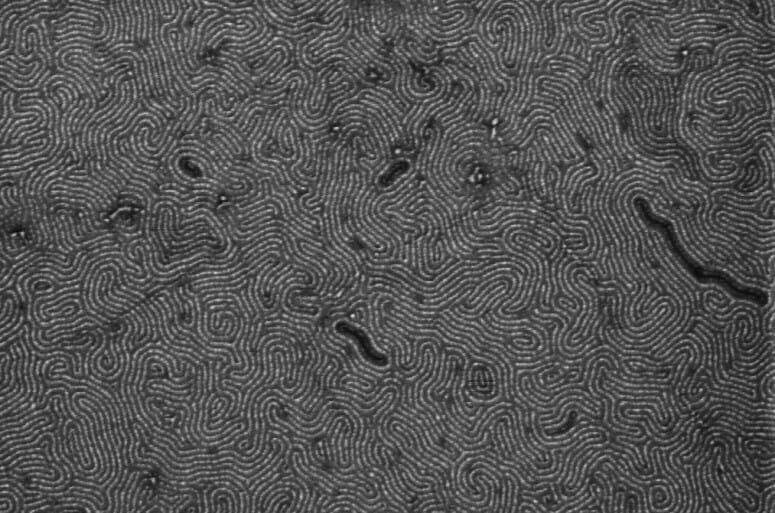
greyscale scanning electron micrograph of graphene nanoribbons that looks like an intricate fingerprint. has also been described as a "zen garden"

From radio to television to the internet, telecommunications transmissions are simply information carried on light waves and converted to electrical signals.

Joel Siegel

Silicon-based fiber optics are currently the best structures for high-speed, long distance transmissions, but graphene — an all-carbon, ultra-thin and adaptable material — could improve performance even more.

In a study published April 16 in ACS Photonics, University of Wisconsin–Madison researchers fabricated graphene into the smallest ribbon structures to date using a method that makes scaling-up simple. In tests with these tiny ribbons, the scientists discovered they were closing in on the properties they needed to move graphene toward usefulness in telecommunications equipment.

“Previous research suggested that to be viable for telecommunication technologies, graphene would need to be structured prohibitively small over large areas, (which is) a fabrication nightmare,” says Joel Siegel, a UW–Madison graduate student in physics professor Victor Brar’s group and co-lead author of the study. “In our study, we created a scalable fabrication technique to make the smallest graphene ribbon structures yet and found that with modest further reductions in ribbon width, we can start getting to telecommunications range.”

For the full story, please visit: https://news.wisc.edu/flexible-easy-to-scale-nanoribbons-move-graphene-toward-use-in-tech-applications/